m: +48 33 874 98 00

e-mail: office@fideltronik.com

Electronic circuit design in the design-for-manufacturing model

The quality of designs in electronics depends on many factors. The experience of the ODM company providing such services, and its ability to apply good practices in design for manufacturing and design for testing are crucial. We explain how electronic circuit design works in the Fideltronik Group.

The Polish electronics manufacturing market is developing very dynamically. The range of services offered by domestic providers is also growing. In addition to manufacturing and assembling printed circuit boards, domestic EMS providers are more and more often offering original design manufacturing (ODM), prototyping, testing and validation.

It should be remembered that a key role in the design and manufacture of electronics is played by quality which is the result of the market experience of companies providing such services. In the Fideltronik Group, the design office has been operating since 1996 and is closely linked to the R&D department which brings together the best professionals.

Original design manufacturing (ODM) in cooperation with the R&D department

– Our design office currently employs more than 70 people, mostly electronic and embedded software engineers. We also have a mechanical department, a prototyping department, and a dedicated team for project quality control and validation. Everything is supervised by project managers who are also responsible for the first contact with our customers,” says Mariusz Osowski, director of the R&D department in the Fideltronik Group.

Like our R&D department, the project office is divided into competence teams. These bring together specialists in areas such as energy conversion, lighting technologies, the Internet of Things or broader innovations that require interdisciplinary skills. This structure ensures a better flow of knowledge and greater working efficiency.

Some projects are assigned to individual groups of professionals. The more complex ones are carried out by multi-skilled teams. Depending on the requirements, these may include embedded software specialists or mechanical engineers, for example. In turn, the validation team joins the project at the testing stage. Each project is overseen by a project manager who is also responsible for the relationship with the customer.

Electronic circuit design – a bespoke approach

The way we work on ODM projects depends largely on the degree of detail of the customer’s requirements are. – Some of the jobs we do are strictly defined. So much so that even the number and colour of the wire bundles are listed. In this situation, we simply follow the specification,” explains Osowski. In some cases, however, customers come in with a loosely sketched concept and ask for help in specifying it and estimating the project cost and time. We then usually offer a feasibility study which allows us to refine the requirements bearing in mind the customer’s business objectives.

– Thanks to our many years of experience, we are able to propose optimum solutions. The customer accepts or rejects individual proposals until a concrete vision of the project can be developed and the key requirements can be itemised,” explains the head of the design office. The feasibility study gives a realistic shape to the initial concept, clarifies it and helps determine the full project cost which includes not only development (the process of designing the electronic circuit), but also additional expenses related to certification and implementation in the production of the final device – up to the stage when it leaves the factory.

ODM + EMS. Combining electronics design with manufacturing pays off

ODM services are usually provided in conjunction with electronics manufacturing services (EMS). However, there are times when customers are only interested in doing the design and outsource the manufacturing to another company. We also take on such work as we are able to design devices within the process window of most EMSs. However, dividing the process between two independent companies makes it difficult to estimate the costs.

Customers who opt for design and assembly within the Fideltronik Group can count on a comprehensive project pricing: from the execution study to the implementation costs. In addition, thanks to our extensive manufacturing knowledge and close contacts with the production department, we are able to offer better cost optimisation right from the design creation stage.

Design for manufacturing, design for testing: designs optimised for manufacturing and testing

– We design electronic devices according to the standards of design for manufacturing (DFM), or what is known as producibility, and design for testing (DFT). These are intended to give the product a set of features that enable it to be easily manufactured at low cost under specific manufacturing conditions, followed by effective testing,” explains Osowski.

This approach requires a great deal of experience and the ability to take into account the many variables that affect the production process. Some ODMs and EMSs offer seemingly cheaper solutions, but these may end up costing more in the long run. On the other hand, it is sometimes worth spending more upfront to avoid complications and reap greater benefits at the product launch stage.

The Fideltronik Group has complete technological facilities for testing and validation

Verification and validation play a key role in the design of electronic circuits. These are tedious processes that usually take as much time as development itself. It is worth noting that the design process itself should not take longer than testing – if it does, it has been poorly planned. Due to the rapid pace of technological progress, market requirements and competitive pressures, the design process including full validation in external laboratories should be completed within a maximum of one and a half years. Maintaining the right pace is accelerated by the appropriate selection of reproducible (“reusable”) solutions at the initial development stage, as well as the availability of appropriate technological facilities.

– The Fideltronik Group is one of the few companies in the industry to have its own electromagnetic compatibility (EMC) test laboratory, equipped with an anechoic chamber and environmental chambers. This allows us to perform up to 95 per cent of our tests on site,” says Osowski. It should be noted that the effectiveness of the verification of designed solutions depends not only on the appropriate infrastructure, but also on the experience of the company performing such tests. Reliable validation of electronic equipment is essential for obtaining certificates that allow access to the markets of the European Union (CE) or the United States (FCC).

Wide range of ODM projects: from energy conversion to monitoring systems

As part of the project office, we carry out a wide range of projects. Today, more than half of them are related to energy conversion. This is an area in which we can have exceptional expertise: for many years we have had an established position in the uninterruptible power supply (UPS) market. We are particularly proud of our drivers (power supplies) for 2000 Watt stadium lighting. When we started manufacturing these units in 2015, we were the only company in the world able to manufacture them to customer specifications. Today, these units are not only used in stadiums, but also in road tunnels and airports, including in Germany.

In addition to power systems as an ODM business, we have many other projects to our credit, such as a motherboard for a food processor, a welding machine, air pollution sensors or a device to monitor a driver’s driving style. – As well as designing from scratch, we also verify finished solutions at our customer’s request. We are able to accurately assess the functionality of the designed product, the production costs, the possibility of further product optimisation or the costs in line with design-for-manufacturing recommendations, as well as help the customer get the product manufactured,” says Osowski.

Design, manufacture, tests – we support all stages of electronics production

We also support customers in the testing processes (FCT/ICT) that are an integral part of product launch, alongside electronic circuit design and manufacturing. We have advanced test facilities and a full range of test equipment. We also know how to test electronics for compliance certificates for selected markets, including Europe (CE) and the USA (FCC), as well as China (CCC).

– We are able to guide the customer through the entire design, test and manufacturing process in such a way as to turn the initial concept into a fully validated device, ready for launch in the customer’s chosen market. We do this by carefully optimising costs, taking into account the overall process and the customer’s business objectives,” concludes Osowski.

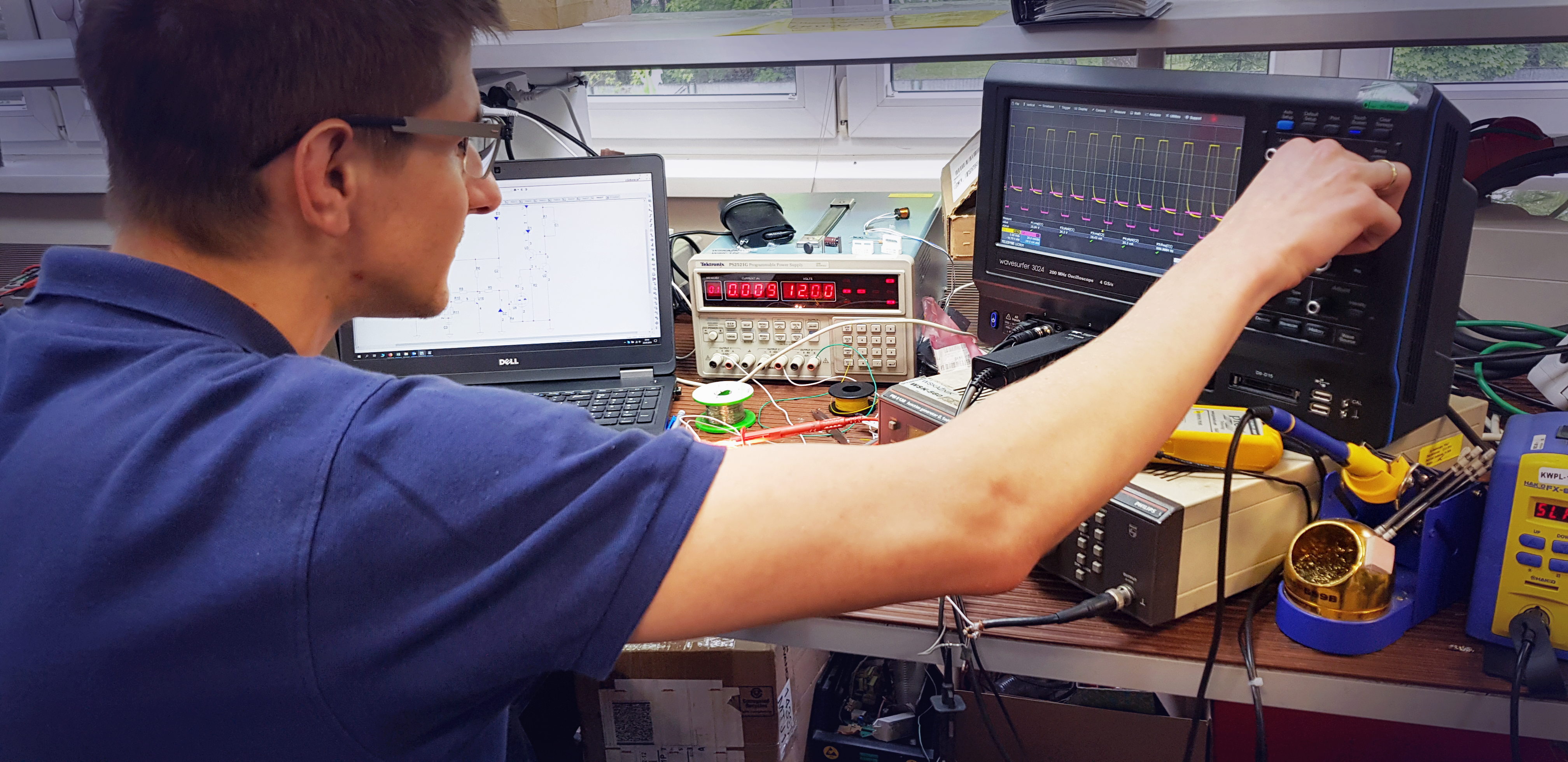
Maximizing Quality, Minimizing Risks: A Short Guide to Electronics Testing

Electronics testing can be a strategic advantage rather than a compliance hurdle. The challenge lies in designing an approach that aligns business goals with cost efficiency.

Electronic products are complex ecosystems that cannot afford shortcomings. A single weakness can lead to cascading failures, safety hazards, or disappointing user experiences.

Imagine a scenario when a seemingly perfect device with a hidden flaw (e.g., overheating, battery issues, etc.) launches well, but user issues occur within a month. Consequences include recalls and repairs, damaged reputation affecting future sales, and potential lawsuits.

Negligence can be painfully costly in electronics design. Flawlessness is all-important and, roughly speaking, depends on two factors: the experience and expertise of a Design House (R&D) or electronics manufacturing services company (EMS) and thorough testing.

How much testing do I need (and can I have less of it)?

Clients focused on speed to market and cost efficiency may want to rush things forward. They expect that RnD experts know their job and can handle things correctly. That’s usually the case, but the complexity of electronics design and risks involved make testing necessary. However, things can be streamlined by setting the proper foundation.

Electronics design starts with communication. The success of a project relies on design thinking and empathy. Designers need to fully understand a client’s requirements and business goals. They may suggest improvements/simplifications or alternative solutions that meet a client’s needs better. They also have to clarify the potential limitations of the solutions under consideration. Only then can things move forward smoothly , and the actual design work may be as effective as possible.

A critical step in the process is creating the test plan followed by the acceptance criteria which provide the benchmarks confirming the client’s requirements market The test plan, including the mentioned acceptance criteria, act as a bridge between the initial concept and the final product, ensuring common understanding.

Depending on the approach or considered scenarios, a test suite can be based on:

  • Quality Testing Plans (QTPs), which outline specific tests, test cases, and methodologies to be used throughout development and production,
  • or Design Verification Plans & Reports (DVP&Rs), which focus on verifying whether the design itself is functional in the system.

Testing plans translate the acceptance criteria into actionable steps for the testing and validation team. They are a critical component of the project’s success, as defined by the client and the contractor. Many R&Ds assume that the scope of testing should more or less equal the development time. It’s frequently the case, but the actual ratio depends on several factors, including:

  • device complexity: simple devices with well-understood technology might require proportionally less testing time compared to complex, cutting-edge devices with novel features,
  • development methodology: testing throughout the development process (agile approach) can reduce the need for dedicated tests at the end,
  • regulatory requirements: devices subject to strict regulations will naturally require more comprehensive testing,
  • and the client’s risk tolerance.

Ultimately, the scope of testing should rely on a thoughtful evaluation of the project’s requirements (including industry standards and legal requirements) and the client’s priorities.

The goals of testing: a breakdown of test types in electronics design

Approaches to testing vary across companies and projects. Based on our over 20 years of experience and thousands of completed projects, we classify electronic device tests into three groups (which may sometimes overlap):

  • functional tests,
  • non-standard (abnormal conditions test / failure tests)
  • and normative, aka conformity tests.

Let’s give them a closer look.

Functional tests

Functional tests ensure that a device meets its specifications and performs reliably under real-world conditions. They can expose hidden issues in the overall design that might not be apparent through individual component testing. This could be anything from compatibility problems between components to unexpected interactions under specific use cases. Properly performed functional tests allow engineers to identify and fix any potential issues before the product’s debut.

Non-standard tests

Non-standard tests prepare the system for „abnormal” conditions. They address exceptional situations that, nevertheless, can’t be ignored. For example, wireless transmission is interrupted. The signal drops out, and the device loses connectivity. The system should respond appropriately, e.g., by displaying an „out of range” message. Such an issue seems simple to handle, but requires specific test scenarios to ensure comprehensive coverage.

Another critical case is testing for safety under non-standard conditions, such as protection mechanisms in devices powered by hazardous voltages. These safeguards must activate when the product sustains damage, preventing severe consequences like fires or electric shocks. Testing under „abnormal” conditions involves simulating physical damage to ensure these protections work effectively, safeguarding both the system and the user.

For example, many have experienced a blown breaker when a device gets damaged or wet. Non-standard tests are essential to verify that the built-in safety features can handle unexpected events, ultimately ensuring the device’s reliability and user safety.

Normative tests

Last but not least, there are normative tests. They ensure a device complies with regulations and industry standards that guarantee safety, performance, and interoperability for electronic products. Clients often require certification from accredited bodies to ensure the device meets specific standards (such as CE, UL, FCC, VDE, ENEC, etc.). The certification process can be lengthy and costly, affecting the product’s time to market.

Fortunately, preliminary tests conducted in-house can streamline things. With an EMC chamber on-premises, a well-equipped laboratory, a team of experienced engineers, and thousands of hours spent addressing electromagnetic compatibility problems, we can offer clients preliminary testing at reasonable times and costs. This can be part of a broader collaboration or provided as expert consultancy. Ultimately, we can guarantee that the device will pass certification smoothly after our preliminary tests, saving time and resources.

Testing is beneficial, but can it also be cost-efficient?

Thorough testing of electronic devices, even at the mock-up stage, provides invaluable insights into potential problem areas, allowing for early intervention and revealing hidden flaws. Such a proactive approach reduces the risk of certification failures, prevents project delays, and increases speed to market, ultimately benefiting a company’s revenue and reputation.

Investing in thorough testing pays off in the long run but requires initial costs. They can be mitigated in several ways, with some already mentioned above. Overall, increasing cost-efficiency involves:

  • transparent communication and setting clear objectives to avoid rework,
  • testing earlier to avoid issues later,
  • conducting preliminary tests in-house,
  • standardization and reuse of testing within a single project (the scope of this approach depends on several factors),
  • test automation – a lengthy topic we’ll cover in another article.

In conclusion, effective electronics testing requires balancing risks and benefits while exploring cost-reduction strategies – all with business goals in mind.

Design For Manufacturing: How To Ensure Smooth Transition To Mass Production

Electronics companies often face production hurdles when scaling up. Leveraging design for manufacturing (DFM) principles early in the design phase can help identify and address potential production issues before they escalate.

Electronic devices are made for profit. No one invests in development to craft a prototype that will gather dust on a shelf. However, transforming a blueprint into a market-ready product is a lengthy and costly process. It involves significant expenses, both direct and indirect.

They include creating the design, component purchases, assembly, logistics, marketing, and more. Recouping costs and reaching profitability may take significant time post-launch. Sometimes, though, the product is an instant smash. Here’s where things get a bit tricky.

Unexpected demand can strain scalability

Fideltronik services various types of clients, ranging from startups to multinational corporations. We also deal with a wide array of projects, some highly innovative and difficult to predict in terms of market reception and profitability. Many of them, though, turn out to be instant hits already at the pilot stage.

For startups, this can be a reason to both celebrate and be concerned. Instead of capitalizing on early success, the company may be unable to accommodate a rapid growth in demand due to scalability limitations.

Challenges may include the following:
– extended production time: if the initial manufacturing process is designed for small-scale production, delays may occur when trying to scale up quickly,
– manual labor: while initially flexible, becomes a constraint as production volumes increase, leading to longer production cycles and higher labor costs,

– testing and quality control: additional testing equipment or personnel may be necessary to ensure new products meet quality standards before shipment,
Additional issues may include supply chain disruptions, limited resources, and lead times for some components.

Many, if not most, of the common issues occurring during a sudden increase in demand may be avoided by applying Design For Manufacturing (DFM) at the early stage of development.

Design for manufacturing: what are the benefits?

Design for manufacturing is an engineering practice of optimizing the design of a product to make it easier and more cost-effective to manufacture. It’s essentially designing with manufacturing capabilities and performance in mind from the very beginning.

Core principles of DFM include:
– simplification: keeping designs simple with fewer parts and easier assembly to minimize production complexity and cost,
– standardization: using common, readily available components to reduce reliance on specialized parts that might be scarce or expensive,

– manufacturability: considering manufacturing rules and process requirements and limitations during design to identify potential issues early,
– testability: designing products for easy and efficient testing to ensure consistent quality control.

DFM has numerous advantages. Most notably in this context, it allows for flexible production volumes, helping companies respond to market changes quickly and efficiently. It also reduces production costs, minimizes waste, ensures consistent results, and helps accelerate time to market by addressing manufacturing hurdles.

DFM helps avoid costly reworks upon moving to mass production

Designing devices for mass production differs significantly from small-scale manufacturing. In the latter case, even minor inefficiencies – such as a slight decrease in yield or a few-second increase in assembly or testing time – can lead to substantial costs.

Products designed without DFM principles may require significant redesigns to meet high-volume production demands. On the other hand, incorporating the DFM review process into the project early on allows companies to avoid much hassle.

Mastering DFM principles might not always fit perfectly within a startup’s agile workflow. Still, the approach can be applied during the prototyping phase (nearly all electronic device projects involve building prototypes), allowing for early adjustments and helping avoid bottlenecks.

Rapid prototyping with Fideltronik

Many of our clients, both current and prospective, are unaware that Fideltronik offers dedicated prototyping services (especially within the R&D department), including rapid prototyping capabilities.

This comprehensive offering helps us verify projects against potential production issues and optimize the manufacturing process. When the prototype is made, our clients receive immediate feedback on current and potential future issues in large-scale manufacturing.

Advantages of integrating DFM early in the process

Simple adjustments can significantly facilitate the production process. Examples include: spacing components differently, moving them to the other side of the PCB, or rotating them by 90 degrees. Such changes benefit not only mass production but also the pilot phase.

Typically, we recommend performing DFM early on, e.g., during the PCB design review or prototyping phase. Such a proactive approach prevents potential manufacturing issues and allows for timely adjustments. Overall, by leveraging DFM, startups can better navigate the transition from pilot to large-scale production, ensuring their innovations reach the market seamlessly and sustainably.

Quality Over Price. How To Avoid Pitfalls In Electronics Design?

Opting for a cheaper price at the expense of quality is a risky strategy in electronics design. EMS companies must prioritize transparency with clients, informing them of potential drawbacks and finding the optimal solution.

In industries where quality is everything, a low price can be a threat / liability rather than a bargain. Clients who prioritize low costs inadvertently expose themselves to long-term risks they may not fully realize. If this is the case, it’s in their best interest to consider finding the right balance between expenses and desired outcomes under expert guidance.

How to approach a project focused on the lowest pricing?

The client is always right. Except when they jeopardize their own business by explicitly wrong decisions, and they can be helped by professional advice.

Obviously, the role of a Design House (RnD) or Original Design Manufacturer (ODM) company is not to provide unwarranted mentoring. Still, an experienced contractor is obliged to cater to the client’s needs with the best intentions possible – even if this entails suggesting significant revisions to the original idea or project.

A common situation where such an intervention is suitable or outright required is when a client emphasizes the cheapest solutions. While keeping costs down is always a desirable goal in electronics design, focusing solely on the lowest pricing can lead to a cascade of problems down the line.

Hence, it’s imperative that a contractor, in the most tactful manner, highlights the trade-offs related to such an approach.

The downsides of the budget-driven design

Every seasoned electronics design expert is familiar with the drawbacks of a cost-centric approach. They include:

– hidden costs and compromised performance: the cheapest components often have higher failure rates and inferior performance specs impacting efficiency, decreasing MTBF and, in the end, negatively affecting the reliability of the final product,

– limited testing: keeping the budget tight may limit the scope of analyses and simulations, impacting reliability (DFMEA) and production costs (DFM/T/A), increasing the number of no-fault-found complaints and servicing costs (DFSS/sensitivity), and lowering the product’s perceived quality,

– compatibility issues: super-cheap components might not integrate seamlessly with other parts of the design, decreasing the product’s parameters and causing , leading to compatibility issues over time, which may require withdrawing the product from the market additional workarounds,

– safety concerns: using low-quality components and simplified solutions might mean cutting corners on safety features and putting users at risk, resulting in product recalls, damaged brand reputation, and even lawsuits,

– maintenance headaches: designs built with cheap components might require more frequent maintenance or repairs, increasing overall costs in the long run.

The list goes on. Fortunately, it can be reduced to zero by proper guidance and putting the project in the right perspective.

Let’s keep things real: full transparency vs overpromising

It’s understandable that clients aim for the best cost-to-value ratio. However, they’re not always aware of the limitations and challenges involved in bringing their ideas into reality.

Many companies expect premium features at standard or low prices. These goals are obviously in contradiction . Premium functionality typically requires high-quality components, complex design features, and potentially advanced manufacturing processes.

An eager contractor trying to appease a client may try to bridge this gap by downplaying potential risks, overpromising on performance, suggesting untested solutions, and failing to convey clear information. Such compromises are dangerous and tend to backfire in the long run.

The number one rule for avoiding disappointments and pitfalls in the electronics design process is to maintain clear communication and full transparency with the client right from the beginning.

Feasibility check

EMS and ODM contractors bring a wealth of experience and knowledge to the table. They can analyze the client’s original ideas and assumptions about functionality, components, and manufacturing processes, providing essential insights and recommendations.

Such a consultation may be an unpleasant reality check for the client. In fact, it protects them from a much bigger disenchantment related to the previously described drawbacks.

A standard measure to prevent mistakes and misunderstandings later in the process is a feasibility study (proof of concept), which assesses the project’s practicality. Such an analysis helps determine if the client’s desired product is achievable within the specified budget.

If not, it explores alternative solutions that best meet their needs. A reasonable approach is to provide a client with a choice of options adjusted for different budget limitations, for example, low-cost, medium-cost, and premium ones.

Functionality and cost optimization based on the client’s feedback

At Fideltronik, the process is fairly straightforward and cost-efficient. Based on our over 20 years of experience in manufacturing energy processing systems, we create functional mock-ups with functional blocks verified in other projects.

We’re able to design the initial model of the device at a relatively low cost to demonstrate how we can solve the problems in question to achieve the client’s goals.

The next step is to collect the client’s feedback and optimize the prototype both feature-wise and cost-wise. The client should be aware of which factors have the biggest impact on the project’s price and production deployment costs.

Strategies to mitigate expenses without compromising quality should also be discussed. Keeping things transparent allows us to minimize the risk of unexpected results during further project stages focused on EMC and thermal tests.

Prioritizing empathy

Focusing on the client’s needs and maintaining clear communication throughout the process is paramount for the project’s success. Approaching clients with empathy helps us better understand their goals, needs, and constraints, contributing to smoother and more efficient cooperation. It also facilitates exploring creative solutions that may overcome the initial limitations.